Embedded Signal
Processing
Project 3: ADC and Clocks
Overview
M.S. students randomized
groups of two each week, never working with same student, unless
otherwise directed by instructor.
Ph.D. students have option to choose their groups (all Ph.D. or
mix), with or without randomization.
The objective of this project is to become familiar with:
NOTE: Use the Project Report Template and see below
for minimum required data content
your reports and demos.
IN NO CASE may code or files or data or pictures be exchanged
between student groups, there is to be NO COPYING of group
reports!
Also, each student must be able to independently
answer any questions themselves during demos.
All students are expected to learn all aspects of every project.
Nevertheless, students are encouraged to collaborate (not copy)
during the lab sessions.
- Some technical notes:
- The FRDMK64F board uses the 100-pin MK64FN1M0VLL12
MCU, with
- maximum operation frequency of 120 MHz, 1 MB of flash, 256
KB RAM,
- full-speed USB controller, Ethernet controller
- 12-bit DAC (see pin DAC0_out on the Arduino header)
- 16-bit ADC (see pins A0 to A5 on the Arduino header)
- 68 GPIO (see pins AD0 to AD15 on the Arduino header)
- The 100-pin package on the FRDMK64F has one DAC module, the 121-pin and
144-pin packages have two DAC modules.
- For more ADC information, see:
Part 1, ADC Programming
- See below for minimum required data
content for your reports and your demos
- In this part, programming the 16-bit ADC on the FRDMK64F using
mbed IDE is investigated
- First, create and run the code as follows:
- Log into your mbed.org
account
- Go to the mbed
compiler view
- Create a new program using Mbed::MenuBar::NewProgram (blue
arrow below) and
- selecting the FRDM-K64F platform,
- gpio example program template,
- and name frdm_adcClks01 (blue circle below) as shown below
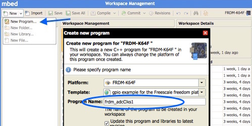
Fig. 1
- Open the Program Folder and double-click main.cpp (blue
arrow below) to open the main program file as shown below
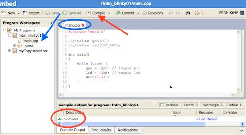
Fig. 2
- Inspect the main.cpp program code (use main.cpp tab in blue
circle above)
- Click the Mbed::MenuBar::Compile button (red arrow above)
- Make sure that you observe
"success" for the compilation at the bottom of the mbed
window, as before
- Also, note that the file "frdm_whateverYourFileName.bin"
should have been downloaded to your computer
- At this point, you have just confirmed that everything is
working normally as in previous projects
- Plug in your FRDM-K64F board
- Create and run the project code as follows:
- Delete any .bin file that was compiled above and downloaded
to your computer, since we will next replace the default
gpio_example with our own code
- Next: edit the code in the main.cpp frame of the mbed
compiler, as follows
#include "mbed.h"
DigitalOut gpo(D0);
DigitalOut led(LED_RED);
AnalogOut dac0out(DAC0_OUT);
AnalogIn adc0in(A0); //A0 = PTB2
int main()
{
uint32_t mask16=1<<16;
uint32_t dat1=(PTC->PDOR) | mask16;
//set Port Data Output Register
uint32_t dat0=(PTC->PDOR) &
(!mask16); //clear
uint16_t tpAdc0in=1;
DAC0->C0 = 0; //reset state
DAC0->C1 = 0;
DAC0->C0 =
DAC_C0_DACEN_MASK // Enable
| DAC_C0_DACSWTRG_MASK // Software Trigger
| DAC_C0_DACRFS_MASK; // VDDA selected
while (true)
{
//example
using write to a single bit, DOarduino=PTC16
(PTC->PDOR)=dat0; //clear
(PTC->PDOR)=dat1; //set
(PTC->PDOR)=dat1; //set
(PTC->PDOR)=dat1;
//set
(PTC->PDOR)=dat1; //set
(PTC->PDOR)=dat0; //clear
tpAdc0in=adc0in.read_u16();
wait((float)(0.001e-6));
DAC0->DAT[0].DATL =
(uint8_t)((uint16_t)(tpAdc0in>>4)
& 0xFF);
DAC0->DAT[0].DATH =
(uint8_t)(((uint16_t)(tpAdc0in>>4) >> 8) &
0x0F);
wait((float)(0.001e-6));
}
}
- Note that the mbed library AnalogIn is being used to access
the ADC. To see this, open the AnalogIn class (red arrow
below)
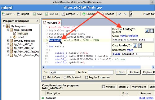
Fig. 3
- Visit mbed-src
to see the details of AnalogIn.h which resides in the mbed
library
- Even more instructive to see AnalogIn.h:
- Export your project as a zip archive using right-click the
program folder in mbed, exportProgram, k64fTarget,
toolchainZipArchiveWithRepositories
- Unzip the archive that is downloaded
- Navigate to the mbed folder to inspect all the header
files and definitions within them
- Next, set up a signal generator in the lab:
- First, onnect the signal generator output to an
oscilloscope
- Connect the "gnd" pin on the signal generator to the
oscilloscope ground clip
- Set the signal generator to a 10 KHz triangle wave, with
offset and peak voltages such that the signal lies between 1
and 2 volts as shown below (Note: different
equipment may require different settings!)
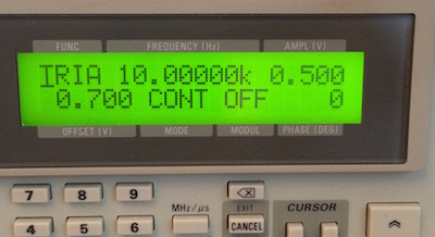
Fig. 4
- Check that the triangle wave is correct, using the
oscilloscope, as follows:
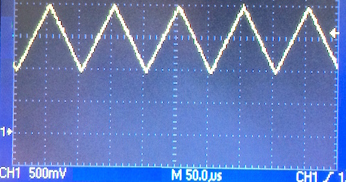
Fig. 5
- Make sure the signal is between 0 and 3 Volts, to avoid damaging your board!
- Plug in your FRDM-K64F board
- Connect the "gnd" pin on the Arduino header to the
oscilloscope ground clip and to the signal generator ground
clip
- Load and run the program that was created above
- Only AFTER you make sure that the
signal is between 0 and 3 volts, connect the signal generator
to Arduino-header pin A0 (PTB2), the 16-bit ADC pin
- Connect the oscilloscope to the DAC output:
- Connect the "gnd" pin on the Arduino header to the channel
2 oscilloscope ground clip
- Connect channel 2 of the oscilloscope to the Arduino
header DAC0_out pin
- Compile and load the program
- Press reset and run the program
- Press the "single" button on the oscilloscope to capture a
single trace as shown below
- You should see a digital signal as follows:
Fig. 6
- What is the sampling frequency of the 16-bit ADC in sample/s
as computed from your oscilloscope trace as illustrated above?
(this is sample rate R1 in your
report)
- If your output looks like the figure above, your circuit is
behaving like a digital amplifier with
gain=1
- Change the gain to 1/2 by modifying your program code,
and plot the new output in your report as the "slow digital amplifier with gain=1/2", and
you must show both traces as above
- Next, determine the relative amounts of time taken by the
ADC conversion and the DAC conversion by using GPIO pins
- Below, the narrow pulse occurs at the beginning of the ADC
conversion, and wide pulse at the end of the conversion
- Edit the code in the main.cpp frame of the mbed compiler, as
follows
#include "mbed.h"
DigitalOut gpo(D0);
DigitalOut led(LED_RED);
AnalogOut dac0out(DAC0_OUT);
AnalogIn adc0in(A0); //A0 = PTB2
int main()
{
uint32_t mask16=1<<16;
uint32_t dat1=(PTC->PDOR) | mask16;
//set Port Data Output Register
uint32_t dat0=(PTC->PDOR) &
(!mask16); //clear
uint16_t tpAdc0in=1;
DAC0->C0 = 0; //reset state
DAC0->C1 = 0;
DAC0->C0 =
DAC_C0_DACEN_MASK // Enable
| DAC_C0_DACSWTRG_MASK // Software Trigger
| DAC_C0_DACRFS_MASK; // VDDA selected
while (true)
{
//example
using write to a single bit, DOarduino=PTC16
(PTC->PDOR)=dat0; //clear
(PTC->PDOR)=dat1; //set
(PTC->PDOR)=dat1; //set
(PTC->PDOR)=dat1; //set
(PTC->PDOR)=dat1; //set
(PTC->PDOR)=dat0; //clear
tpAdc0in=adc0in.read_u16();
(PTC->PDOR)=dat0; //clear
(PTC->PDOR)=dat1; //set
(PTC->PDOR)=dat1; //set
(PTC->PDOR)=dat1; //set
(PTC->PDOR)=dat1; //set
(PTC->PDOR)=dat1; //set
(PTC->PDOR)=dat1; //set
(PTC->PDOR)=dat1; //set
(PTC->PDOR)=dat1; //set
(PTC->PDOR)=dat1; //set
(PTC->PDOR)=dat1; //set
(PTC->PDOR)=dat1; //set
(PTC->PDOR)=dat1; //set
(PTC->PDOR)=dat1; //set
(PTC->PDOR)=dat1; //set
(PTC->PDOR)=dat1; //set
(PTC->PDOR)=dat1; //set
(PTC->PDOR)=dat0; //clear
wait((float)(0.1e-6));
DAC0->DAT[0].DATL =
(uint8_t)((uint16_t)(tpAdc0in>>5)
& 0xFF);
DAC0->DAT[0].DATH =
(uint8_t)(((uint16_t)(tpAdc0in>>5) >> 8) &
0x0F);
wait((float)(0.1e-6));
}
}
- Compile and load the program
- Press reset and run the program
- Move the osciloscope probe channel 1 from the signal
generator to the D0 GPIO line on the Arduino header pin D0
(PTC16)
- Press the "single" button on the oscilloscope to capture a
single trace as shown below
- You should see a digital signal as follows:
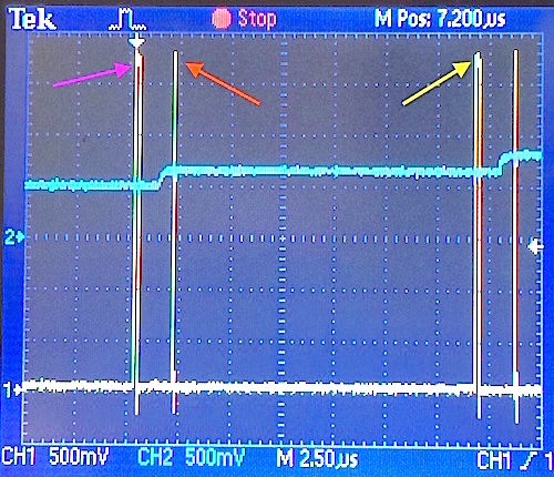
Fig. 7
- What is the ADC conversion time in ns? This is seen as
the time between the narrow pulse (red arrow above) and wide
pulse (yellow arrow above). (this is ADC
conversion time T1 in your report)
- What is the DAC conversion time in ns? This is seen as
the time between the wide pulse (purple arrow above) and
narrow pulse (red arrow above). (this is
DAC conversion time T2 in your report)
- Which is slower conversion time, the ADC or the DAC?
Part 2, Adjusting the System Clocks for Faster ADC Speed
- To adjust system clocks for faster ADC operation, it is
necessary to write to to some registers (low-level code, as
opposed to the mbed-level code)
- But before proceeding, it is helpful to read what the
current clock states/speeds are
- Refer to page 186, Figure 5-1. clocking diagram, in section
5.3 High-Level device clocking diagram of the K64
Sub-Family Reference Manual, Rev. 2, January 2014
- Also refer to page 827, Figure 35-1. ADC block diagram, in
section 35.1 Analog-to-Digital Converter (ADC), of the K64
Sub-Family Reference Manual, Rev. 2, January 2014
- See also page 834 section 35.3.2 ADC Configuration Register
1 (ADCx_CFG1) of the K64
Sub-Family Reference Manual, Rev. 2, January 2014 for
explanations of ADC_CFG1_ADIV(0), ADC_CFG1_ADICLK(0),
ADC_CFG1_MODE(3)
- See page 857 for a table of number of ADC clock cycles (not
the same as MCU clock cycles!) required for conversion
in section 35.4.4.5 Sample time and total conversion time, in
the K64
Sub-Family Reference Manual, Rev. 2, January 2014
, use 25 ADC cycles as a rough guess, if no averaging
- Faster ADC speed will be accomplished by using lower-level
code to write directly to the ADC setup and clock registers
- We will directly set the ADC Registers:
- The variable ADC0 is a pointer to the ADC base
address, and is described in MK64F12.h
- To see MK64F12.h :
- Export your project as a zip archive using right-click
the program folder in mbed, exportProgram, k64fTarget,
toolchainZipArchiveWithRepositories
- Unzip the archive that is downloaded
- Navigate to the mbed/TARGET_K64F folder to inspect the
header file and definitions within
- ADC0 corresponds to memory location 0x4003B000 (seeADC
memory map table in section 35.3 on page 829 of the K64
Sub-Family Reference Manual, Rev. 2, January 2014)
- Next: edit the code in the main.cpp frame of the mbed
compiler, as follows
#include "mbed.h"
DigitalOut gpo(D0);
DigitalOut led(LED_RED);
AnalogOut dac0out(DAC0_OUT);
AnalogIn adc0in(A0); //A0 = PTB2
Serial pc(USBTX, USBRX);
int main()
{
if(1){
uint32_t div1=0,div2=0,busClk=0,adcClk=0;
SystemCoreClockUpdate();
pc.printf("SystemCoreClock= %u
\r\n",SystemCoreClock);
div1=( (SIM->CLKDIV1) &
SIM_CLKDIV1_OUTDIV1_MASK)>>SIM_CLKDIV1_OUTDIV1_SHIFT;
div1=1+div1;
div2=1+( (SIM->CLKDIV1)
&
SIM_CLKDIV1_OUTDIV2_MASK)>>SIM_CLKDIV1_OUTDIV2_SHIFT;
busClk=SystemCoreClock*div1/div2;
pc.printf("Divider1== %u div2=%u
\r\n",div1,div2);
pc.printf("MCGOUTCLK= %u, busClk = %u
\r\n",SystemCoreClock*div1,busClk);
ADC0->SC3 &=
~ADC_SC3_AVGE_MASK;//disable averages
ADC0->CFG1 &=
~ADC_CFG1_ADLPC_MASK;//high-power mode
ADC0->CFG1 &= ~0x0063 ; //clears
ADICLK and ADIV
ADC0->CFG1 |= ADC_CFG1_ADIV(1); //divide
clock 0=/1, 1=/2, 2=/4, 3=/8
if (((ADC0->CFG1)& 0x03) == 0)
adcClk =
busClk/(0x01<<(((ADC0->CFG1)&0x60)>>5));
if (((ADC0->SC3)& 0x04) != 0) adcClk
= adcClk/(0x01<<(((ADC0->SC3)&0x03)+2));
pc.printf("adcCLK= %u \r\n",adcClk);
}
uint32_t mask16=1<<16;
uint32_t dat1=(PTC->PDOR) | mask16;
//set Port Data Output Register
uint32_t dat0=(PTC->PDOR) &
(!mask16); //clear
uint16_t tpAdc0in=1;
DAC0->C0 = 0; //reset state
DAC0->C1 = 0;
DAC0->C0 =
DAC_C0_DACEN_MASK // Enable
| DAC_C0_DACSWTRG_MASK // Software Trigger
| DAC_C0_DACRFS_MASK; // VDDA selected
while (true)
{
//example
using write to a single bit, DOarduino=PTC16
(PTC->PDOR)=dat0; //clear
(PTC->PDOR)=dat1; //set
(PTC->PDOR)=dat1; //set
(PTC->PDOR)=dat1; //set
(PTC->PDOR)=dat1; //set
(PTC->PDOR)=dat0; //clear
tpAdc0in=adc0in.read_u16();
(PTC->PDOR)=dat0; //clear
(PTC->PDOR)=dat1; //set
(PTC->PDOR)=dat1; //set
(PTC->PDOR)=dat1; //set
(PTC->PDOR)=dat1; //set
(PTC->PDOR)=dat1; //set
(PTC->PDOR)=dat1; //set
(PTC->PDOR)=dat1; //set
(PTC->PDOR)=dat1; //set
(PTC->PDOR)=dat1; //set
(PTC->PDOR)=dat1; //set
(PTC->PDOR)=dat1; //set
(PTC->PDOR)=dat1; //set
(PTC->PDOR)=dat1; //set
(PTC->PDOR)=dat1; //set
(PTC->PDOR)=dat1; //set
(PTC->PDOR)=dat1; //set
(PTC->PDOR)=dat0; //clear
//wait((float)(0.1e-6));
DAC0->DAT[0].DATL =
(uint8_t)((uint16_t)(tpAdc0in>>4)
& 0xFF);
DAC0->DAT[0].DATH =
(uint8_t)(((uint16_t)(tpAdc0in>>4) >> 8) &
0x0F);
//wait((float)(0.1e-6));
}
}
- Compile and load the program
- To see the terminal output from the printf()
statements, you must connect a TTY terminal to the FRDM-K64F
- On a Mac, you can use the screen command as follows:
- First, open a terminal on the Mac
- Find the TTY using the command: ls /dev |grep usb
- Start the TTY using the command (yellow circle below): screen
/dev/tty.usbmodem1412 9600screen /dev/tty.usbmodem1412
9600
- Press reset and run the FRDM-K64F program
- An example MAC session may look like the following:
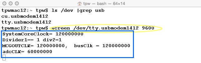
Fig. 8
- Note the terminal printf() output from
your program (blue box above)
- For a PC or linux, To connect a TTY terminal to your
FRDM-K64F on a PC or Linux,
- Press reset and run the program
- Move the oscilloscope probe channel 1 back to the signal
generator
- Press the "single" button on the oscilloscope to capture a
single trace as shown below
- You should see a digital signal as follows:
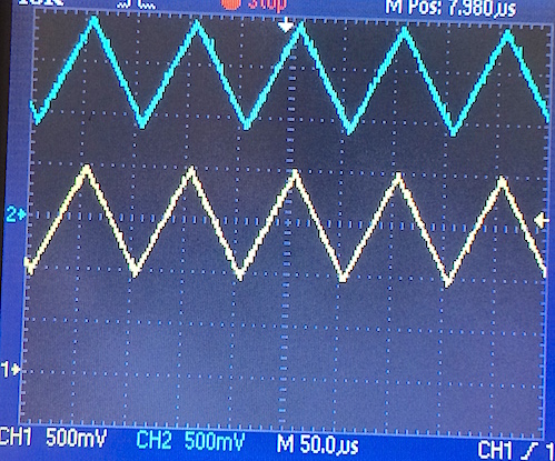
Fig. 9
- Compare Fig. 9 to Fig. 6, and note that the individual
samples are nearly invisible now, since the sample rate is so
high
- Move the oscilloscope probe channel 1 from the signal
generator to the D0 GPIO line on the Arduino header pin D0
(PTC16)
- Press the "single" button on the oscilloscope to capture a
single trace as shown below
- You should see a digital signal as follows:
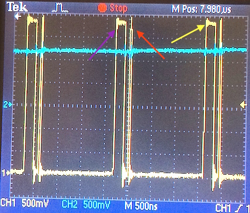
Fig. 10
- Compare Fig. 10 to Fig. 7, noting that the ADC conversion
time has greatly decreased
- What is the ADC conversion time in ns? This is seen
as the time between the narrow pulse (red arrow above) and
wide pulse (yellow arrow above). (this is
ADC conversion time T3 in your report)
- What is the DAC conversion time in ns? This is seen
as the time between the wide pulse (purple arrow above) and
narrow pulse (red arrow above). (this is
DAC conversion time T4 in your report)
- Which is slower, the ADC or the DAC?
- Can you make the ADC run any faster?
- Is the above ADC speed violating rules for maximum ADC
limits for the K64F?
Report Data
- Minimum required data content for
your report and demos
- Required theory content:
- For the gain=1 digital amplifier of Fig. 6, show an
equation for the predicted quantization noise of the digital
amplifier as seen at the output. Consider the
quantization noise contributions of both the 12-bit DAC and
the16-bit ADC in your theory. Compute the
gain1-digital-amplifier output quantization noise Vq in
microvolts.
- Required software code excerpt content:
- Main.cpp code to do the slow mbed-level gain=1/2 digital
amplifier similar to Fig. 6 (just the while-loop portion of
code)
- Required tabular data content:
- The values for:
- Theoretical Gain1-digital-amplifier output quantization
noise Vq in microvolts.
- Measured AnalogIn default sample
rate R1 in samples/second as defined above
- Measured Slow ADC conversion time
T1 in microseconds as defined above
- Measured Slow DAC conversion time
T2 in microseconds as defined above
- Measured Fast ADC conversion time
T3 in microseconds as defined above
- Measured Fast DAC conversion time
T4 in microseconds as defined above
- Required pictures/photos content:
- Legible picture (if pdf of your report is
"zoomed/magnified") showing ADC input and DAC output
voltages for mbed-level slow 1Vpp input 10KHz triangle wave
"slow digital amplifier with gain=1/2"
similar to Fig. 6 above
- Legible picture (if pdf of your report is
"zoomed/magnified") showing GPIO and DAC output voltages for
mbed-level Fast ADC and GPIO pulses as in Fig. 10
- Legible picture (if pdf of your report is
"zoomed/magnified") showing terminal printf output as in
Fig. 8 inside the blue box
- Project Demos
- Be prepared to demonstrate and discuss items such as:
- Demonstrate a low-level fast ADC
- Demonstrate an mbed-level slow ADC
- Change the clocks
- Discuss the data rate
- Demonstrate a gain=1/4 fast or slow digital amplifier
- Change the setup for ADC
- Be prepared to answer questions such as:
- Demonstrate a full clean/build
- What port number is D0 (PT???)
- What port number is D5 (PT???)
- What is a header file?
- What is ADC0->CFG1?
- What is ADC0->SC3?
- What is the base address of ADC0?
Report:
- See above project description for required
report data content.
- NOTE Report Template Use the Project Report Template
( embDspProjTemplate.docx) for your report.
- One pdf-format must be emailed to the instructor at the
beginning of the class meeting of the demo.
- One hardcopy per student, plus
one extra hardcopy for the instructor, should be brought to
class for the demo.
- Do not add extraneous pages or put explanations on separate
pages unless specifically directed to do so. The instructor will
not read extraneous pages!
- YOU MUST ADD CAPTIONS AND FIGURE NUMBERS TO ALL FIGURES!!
Copyright 2015 T. Weldon
Freescale, Kinetis are registered trademarks of Freescale
Semiconductor, Inc. Texas Instruments, TI, C2000, and
Code Composer Studio are a registered trademarks of Texas
Instruments Incorporated. Adafruit is a registered
TradeMark of Limor Fried. ARM, Cortex and Keil are
registered trademarks of ARM Limited (or its subsidiaries).
Apple, Yosemite, Mac OS, iPhone, iPad, MacBook, Mac, iTunes, and
Xcode are trademarks of Apple inc. All other product or service
names are the property of their respective owners. Arduino
is a registered trademark of Arduino.