Microwave Circuits and
Metamaterials
Project 9
Overview
Remain in same project groups for the
semester.
The objective of this project is to investigate waveguide and
metamaterial structures in HFSS software.
NOTE: Use the Project Report Template and keep answers to questions on consecutive sheets
of paper with all plots at the end.
IN NO CASE may code or files be exchanged between students, and
each student must answer the questions themselves and do their own
plots, NO COPYING of any sort! Nevertheless, students are
encouraged to collaborate in the lab session.
Only turn in requested plots ( Pxx )
and requested answers to questions ( Qxx ).
Part 1
- In this part, investigate waveguide and metamaterial
structures are investigated using HFSS software.
- In this part, you will construct a waveguide and measure its
S-parameters and cutoff frequency
- Log into a linux termnal
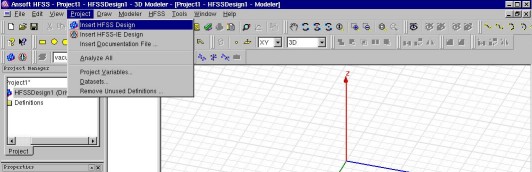
- Run Mosaic::Engineering::Electrical::HFSS
- MenuBar::Project::InsertHFSSdesign as illustrated below
- MenuBar::HFSS::SolutionType::DrivenModal and NetworkAnalysis
- MenuBar::Modeler::Units select mm
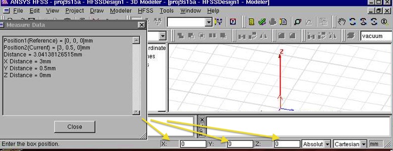
- Next draw the waveguide as a box: MenuBar::Draw::Box
And at the bottom of the screen enter x=0 y=0 z=0 mm,
(yellow arrows below) and then type "enter "or "carriage
return" then type dx=100 dy=22.9 dz=10.2 mm, and then
type "enter "or "carriage return"
- Alterntively, click the DrawBox tool icon (yellow arrow
below), draw any box, click the "createBox" item (red arrow
below), and edit the properties (blue arrow below) to set the
Position=(0,0,0) and dimensions dx=100 dy=22.9 dz=10.2 mm as
given above.
- Press the "fitAll" toolbar item (orange arrow below) to view
the object.
when done it should look like:
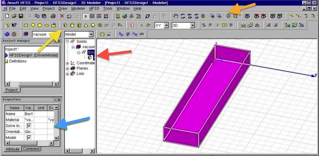
- Save a snapshot of the waveguide as above and paste it into
your report. ( P1 )
- Make sure that your
plots, component
values,
legends, axes, and fonts are legible in your report!
- MenuBar::View::FitAll::AllViews
- MenuBar::Edit::Select::Object then right-click the
waveguide and AssignMaterial air
MenuBar::Edit::Select::Faces then right-click the long
waveguide top face,
then right-click nextBehind to get the bottom plate, then
right-click assignBoundary Perfect-E
and repeat this for the long top face.
In the same fashion assign the two long sidewalls as
Perfect-E boundaries.
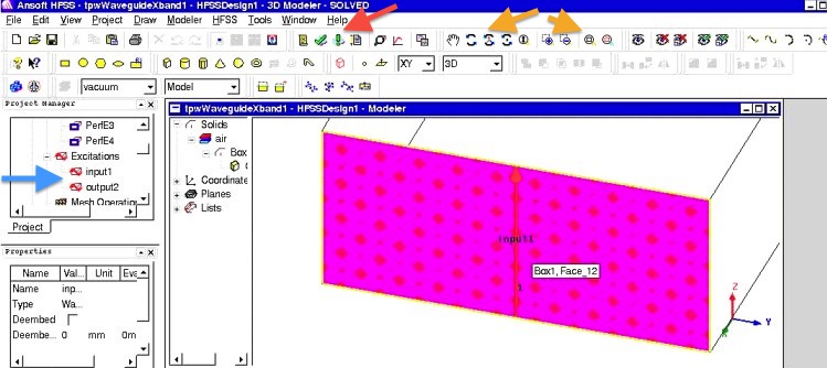
- Right-click the front face, and AssignExcitation::WavePort,
set name=input1,
next, numberofmodes=1, click on the integration line field and
select newline,
and draw a line (yellow circle below) from the center bottom of
the port to the center top of the new port as in the example
below,
click next, donot renormalize, and finish. Repeat this for
the output port.
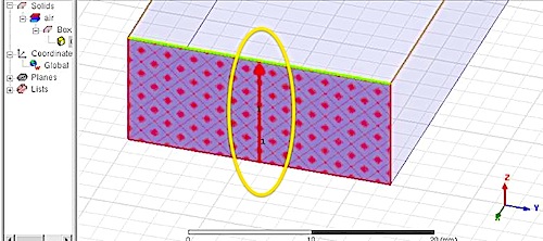
- Highlight the excitation ports in the ProjectManger pane
(blue arrow below)
The ports and integration line should look like:
- The toolbar icons can be used to move the view (orange
arrows above)
- Save a snapshot of the one port as above and paste it into
your report. ( P2 )
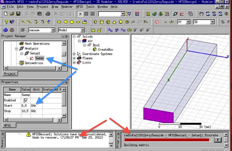
- Next, set up the analysis
- MenuBar::HFSS::AnalysisSetup::AddSolutionSetup select
General::
SolutionFrequency 20 GHz, click OK
- MenuBar::HFSS::AnalysisSetup::AddFrequencySweep and linear
step sweep 6.0 to 16 GHz in 0.10 GHz steps, and SweepType=discreet
- Your analysis and sweep should appear in the
ProjectManager pane (blue arrow below), where the sweep
properties should appear when the Sweep item is highlighted
- Save your work, MenuBar::File::Save
- MenuBar::HFSS::ValidationCheck and Everything should
check OK
- MenuBar::HFSS::AnalyzeAll (red arrow above) to run the
simulation
- Watch for any errors at the bottom message areas (red arrows
below)
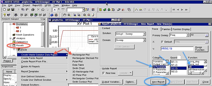
- To see the results, runright-click Results (red circle
below) select CreateModalSolutionDataReport::RectangularPlot
(red arrows below)
- In the popup, select Sparameters::s21::dB (blue arrows
below) and click newReport (blue circle below)
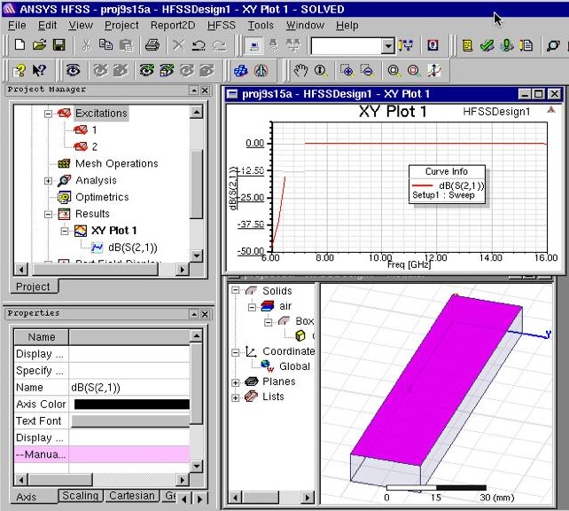
- You should see your s21 plot as below
- To plot the results you may need to click a minimize icon to
show plots/reports hidden behind the top plot/report
- Adjust your plot to go from -50
to 10 dB and double click the lines and make the width=3
- Make sure that the legend does not obscure any portion of
your plotted curves (move it as above).
- Save a snapshot of the s21 plot as above, and paste it into
your report. ( P3 )
- Based on the dimensions
of the waveguide, what size waveguide is this (i.e.,
wr22,wr51,etc? ( Q1 ) Hint http://en.wikipedia.org/wiki/Waveguide_(electromagnetism)
- What is the theoretical cutoff frequency of the lowest-order
mode for the waveguide? ( Q2 )
- At what frequency do you observe that S21 is approximately
14 dB below its maximum value? (
Q3 )
Part 2
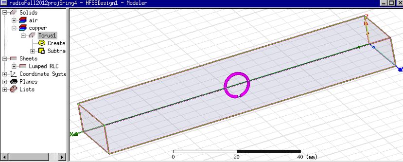
- Save a snapshot of the design as above and paste it into
your report. ( P4 )
- Select the Boundaries::perfectH in the project manager pane
on the left side of the HFSS window, and note that these are the short walls of
the waveguide. The perfectH
boundary is similar to perfectE boundary.
PerfectE is a perfect conductor that does not allow tangential
electric fields at the boundary. PerfectH is a perfect
magnetic conductor that does not allow tangential magnetic
fields at the boundary.
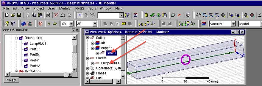
- What is the radius of the ring? ( Q4 )
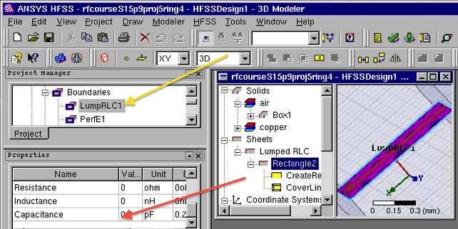
- Zoom in to the gap in the ring by selecting
Sheet::LumpedRLC::Rectangle2 (blue arrow below) and zooming in
(red arrow below) to zoom into the sheet (yellow arrow below)
that is placed in the gap. This "RLC" sheet is
used as a capacitor in the gap.
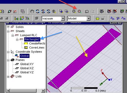
- Use MenuBar::Modeler::Measure::Position to measure the gap
length by measuring the length of the sheet in the gap.
Click one end of the sheet, and observe the distance as you
move the mouse
- What is the length of the gap in the ring? ( Q5 )
- Select the Boundaries::LumpRLC1 item in the project manager
(yellow arrow below) and observe the capacitance of the sheet
in the gap (red arrow below)
- What is the capacitance of the lumped RLC sheet in the gap?
( Q6 )
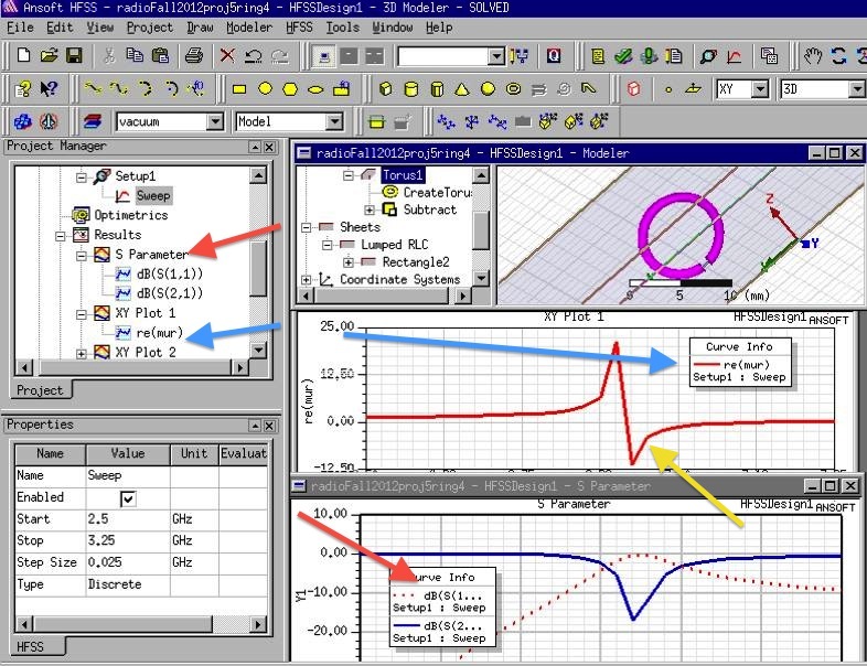
- Run the simulation
- When the simulation completes, select the first two results
plots as illustrated below.
- Plot the relative
permeability as shown (blue arrows below) by
double-clicking XYplot1
- Plot the S-parameters S11 and S21 as shown (red arrows
below) by double-clicking "Sparameter"
- Note the frequency range where the
relative permeability is negative (yellow arrow
above).
- This is the desired metamaterial
behavior.
- Save a snapshot of the S-parameter plot as above, but with
all scales/axes visible, and paste it into your
report. ( P5 )
- Using the equation
for a circular loop here, what is the theoretical
inductance of the ring? ( Q7
)
- Based on the capacitance of the lumped RLC sheet in the gap,
and the inductance from the previous question, what is your
computed value of the resonant frequency is f0=1/{ 2 pi
sqrt(LC) }? ( Q8 )
- Click the ReMuEps plot (red arrow and red circles below) to
plot extracted permittivity and permeability as shown below
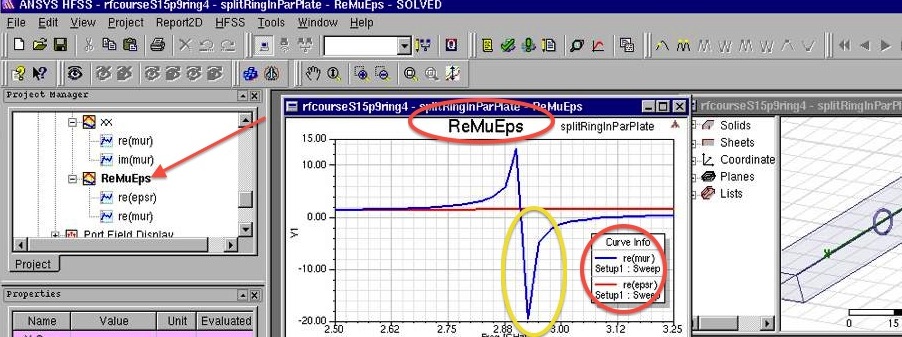
- Save a snapshot of the relative permeability and
permittivity as shown above, but with all scales/axes visible,
and paste it into your report. ( P6 )
- Note the region of negative permeability (yellow circle
above)
- From the capacitance value of the lumped RLC, and from the
frequency of the resonance in the S-parameters, compute the
inductance of the ring that resonates with the capacitance of
the lumped RLC. ( Q9 )
- What are the real parts of relative permeability (mur) and
relative permittivity (epsr) at the lowest frequency (2.5 GHz)
in the plot? ( Q10 )
- What are the real parts of relative permeability (mur) and
relative permittivity (epsr) at the lowest frequency (3 GHz)
in the plot? ( Q11 )
- Note, by right clicking results (in upper left pane of above
figure near red arrow) and selecting output variables, you can
see the formulas used to extract the mu and epsilon (generally
these are approximations below), See http://ieeexplore.ieee.org/xpls/abs_all.jsp?arnumber=1210783
for details on the formulas:
- dd = .01 (length in meters of the physical region
being characterized, typically the diameter of the ring)
- v1 = S(1,1)+S(2,1)
- v2 = S(2,1)-S(1,1)
- k0 = 6.28*Freq/3e8
- mur = 2/(cmplx(0,1)*k0*dd)*(1-v2)/(1+v2)
- epsr = mur+2*cmplx(0,1)/(k0*dd)
- epsr2 =
2/(cmplx(0,1)*k0*dd)*(1-v1)/(1+v1)
- Note: above formulas should be used when de-embedding is
up to within approx 1mm of edge of ring. To see
de-embedding, select Excitation in the upper left pane,
select the waveport, right-click properties, and click the
postprocessing tab. When the waveport is selected, you
should see an 3D arrow indicating how far the results are
deembedded from the waveport.
- De-embedding effectively moves the waveport closer to the
split ring, so the measurement primarily consists of the
effect of the split ring. Otherwise, the measurement
would include the effect of a long portion of empty waveguide
in addition to the effect of the split ring.
- Select Excitation in the upper left pane, select the
waveport, right-click properties, and click the postprocessing
tab. When the waveport is selected, you should see a 3D
arrow indicating how far the results are de-embedded from the
waveport. Save a snapshot showing, but with all
scales/axe the de-embedding arrow, and paste it into your
report. ( P7 )
Part 3
- In this part, you will simulate a simple metamaterial
in a parallel-plate waveguide, a type of split
ring resonator (SRR)
- First, open the split-ring design in wageduide from above
- You will modify this copy to create a parallel-plate
waveguide
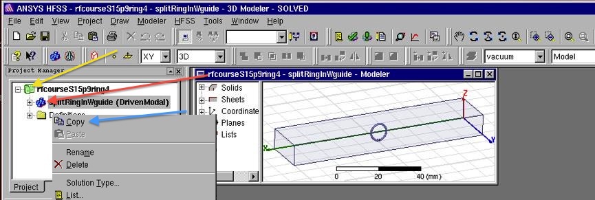
- To make a copy of your previous design:
- Run Mosaic::Engineering::Electrical::HFSS
- Open your previous design with the split ring in waveguide
MenuBar::File::Open
- Right-click the design icon (red arrow below) and select
copy (blue arrow below)
- Right-click the main project folder (yellow arrow below)
and "paste"
- Name the new design "ringParPlate"
- Open the new copy of the design
- Delete the ring and sheet (red arrows below) using
right-click delete
- Insert an i-beam structure
- Draw a first box: MenuBar::Draw::Box And at the
bottom of the screen enter x=50 y=11.5 z=3 mm,
and then type "enter "or "carriage return" then type
dx=0.1 dy=0.1 dz=5.2 mm, and then type "enter "or
"carriage return" Alterntively, click the DrawBox tool
icon , draw any box, click the "createBox" item, and edit
the properties .
- Draw a second box: MenuBar::Draw::Box And at the
bottom of the screen enter x=48 y=9.5 z=1 mm,
and then type "enter "or "carriage return" then type
dx=4 dy=4 dz=1 mm, and then type "enter "or "carriage
return" Alterntively, click the DrawBox tool icon ,
draw any box, click the "createBox" item, and edit the
properties .
- Draw a third box: MenuBar::Draw::Box And at the
bottom of the screen enter x=48 y=9.5 z=8.2 mm,
and then type "enter "or "carriage return" then type
dx=4 dy=4 dz=1 mm, and then type "enter "or "carriage
return" Alterntively, click the DrawBox tool icon ,
draw any box, click the "createBox" item, and edit the
properties .
- Select all three box items and right-click AssignMaterial
as copper
- Draw a rectangle: MenuBar::Draw::Rectangle (if the
non-Model prompt appears, select no you dont want a
non-model object) And at the bottom of the screen
enter x=50 y=11.5 z=2 mm, and then type "enter
"or "carriage return" then type dx=1 dy=0.1 dz=0 mm,
and then type "enter "or "carriage return"
Alterntively, click the DrawBox tool icon , draw any box,
click the "createBox" item, and edit the properties .
- Select the rectangle sheet, and change the orientation to
Y, and zoom in to inspect the sheet (red arrow below) looks
as follows
- Check that everything is OK (red circle below)
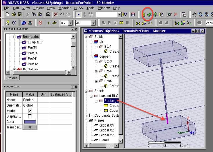
- Select all 3 boxes with control key held down, and zoom in
(blue circle below) so that your view looks like above
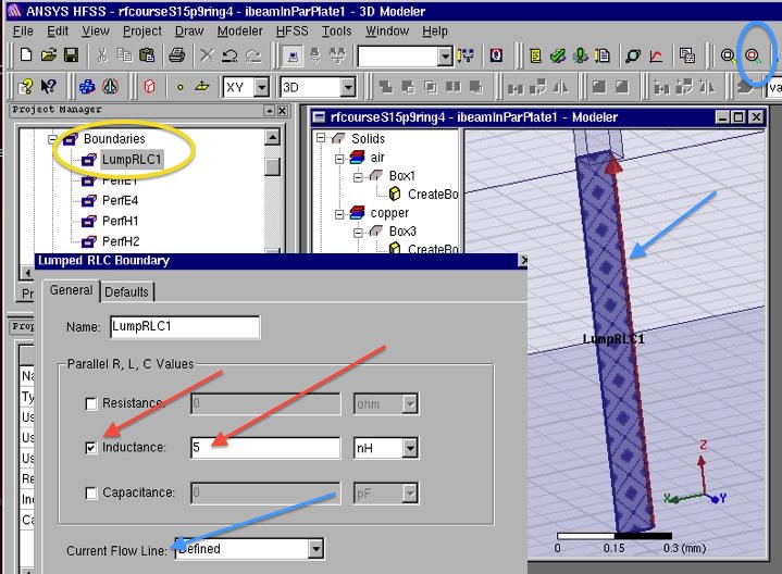
- Select the rectangle sheet (red arrow above), right-click it
AssignBoundary::LumpedRLC
- Save a snapshot of the i-Beam structure as shown above, and
paste it into your report. ( P8 )
- Set inductance to 5 nH (red arrows below)
- Zoom to the sheet (blue circle below) and assign a current
flow line (blue arrows below)
- Select the Boundaries::LumpedRLC1 item (yellow circle above)
and zoom in as shown above to check your RLC sheet
- Save a snapshot of the RLC sheet structure as shown above,
and paste it into your report. ( P9 )
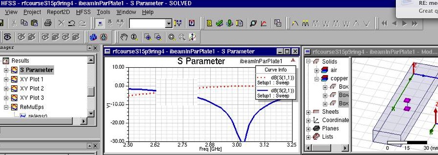
- Run the simulation
- Display the S-parameters as follows
- Save a snapshot of the i-beam S-parameters as shown above,
and paste it into your report. ( P10 )
- Click the ReMuEps plot (yellow arrow below) to plot
extracted permittivity and permeability as shown below
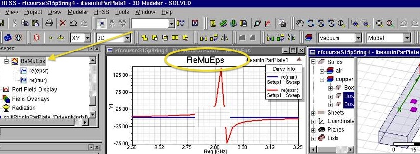
- Save a snapshot of the i-beam relative permeability and
permittivity as shown above, but with all scales/axes visible,
and paste it into your report. ( P11 )
- In the project manager pane on the left, select
Boundaries::PerfectH and delete the two perfectH boundaries
associated with the short walls of the waveguide
- Select the face of the short waveguide wall on the right
using MenuBar::Edit::Select::Faces
- Right-click the selected face and AssignBoundary::PrefectH
to set a perfect-H boundary
(perfect magnetic conductor)
- The perfectH boundary is similar to perfectE boundary.
PerfectE is a perfect conductor that does not allow tangential
electric fields at the boundary. PerfectH is a perfect
magnetic conductor that does not allow tangential magnetic
fields at the boundary.
NOTE ReportTemplate: Use the Project Report Template
and keep answers to questions on
consecutive sheets of paper with all plots at the end.
Do not add extraneous pages or put explanations on separate
pages unless specifically directed to do so. The instructor will
not read extraneous pages!
Only turn in requested plots (Pxx )
and requested answers to questions (Qxx ).
All plots must be labeled P1, P2, etc. and all questions must be
numbered Q1, Q2, etc. YOU MUST ADD CAPTIONS AND FIGURE
NUMBERS TO ALL FIGURES!!
Copyright 2010-2015 T. Weldon
Cadence, Spectre and Virtuoso are registered trademarks of
Cadence Design Systems, Inc., 2655 Seely Avenue, San Jose, CA
95134. Agilent and ADS are registered trademarks of Agilent
Technologies, Inc.