Microwave Circuits and
Metamaterials
Project 13
Overview
Remain in same project groups for the
semester.
The objective of this project is to investigate BJT and CMOS
non-Foster circuits using the ADS simulator.
NOTE: Use the Project Report Template and keep answers to questions on consecutive sheets
of paper with all plots at the end.
IN NO CASE may code or files be exchanged between students, and
each student must answer the questions themselves and do their own
plots, NO COPYING of any sort! Nevertheless, students are
encouraged to collaborate in the lab session.
Only turn in requested plots ( Pxx )
and requested answers to questions ( Qxx ).
Part 1
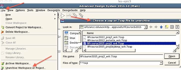
- Load and run the BJT non-Foster circuit example as follows:
- This project does not seem to function
properly when downloaded as a zip-file, so it must be
downloaded as a 7zap archive as follows:
- Download the 7zap archive RFcourse2015_proj13nonFos_wrk.7zap
to your ~/apps/ads directory
- Use MenuBar::File::Unarchive to extract the project into
your ADS directory as below
- You should find a new directory
RFcourse2015_proj13nonFos_wrk created in apps/ads
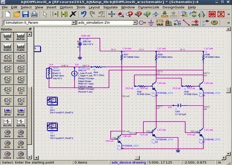
- Go down through the directory tree to bjtDiffLinvill_a and
double click that design file, and the following
schematic should appear.
- Run the simulation, and annotate the
dc voltages on the schematic, using
MenuBar::Simulate::AnnotateDc. Save a snapshot of
the schematic and paste it into your report.
( P1 )
- Make sure that your
plots, component
values,
legends, axes, and fonts are legible in your report!
- For snapshots use the
Linux menu Graphics::Ksnapshot and select the option
to take a legible snapshot of a window rather than full screen
- The BJT transistors are BFP280W, what is the typical
transition frequency, fT, of
this device from the datasheet?
( Q1 )
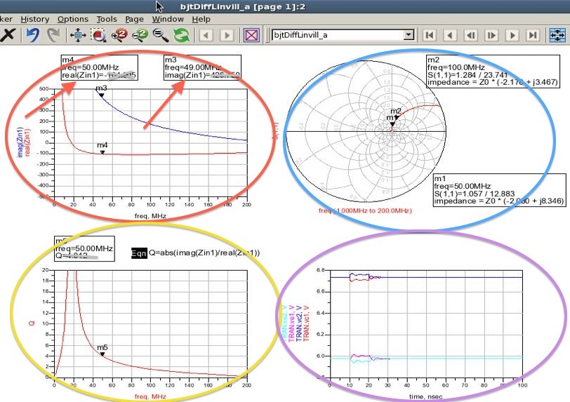
- Run the simulation
- You should see a number of plots as follows:
- Save a snapshot of the real and imaginary parts of Zin (red
circle above), also with 2 markers (red
arrows) at 50 MHz as illustrated
above. ( P2 )
- Does the imaginary part of input impedance Zin1 in the red
circle above follow the proper shape for a negative
capacitor? yes/no ( Q2 )
- What is the real part of input impedance Zin1 at 50 MHz (red
arrows above)? ( Q3 )
- What is the imaginary part of input impedance Zin1 at 50 MHz
(red arrows above)? ( Q4 )
- What is the quality factor of the input impedance Zin1 at 50
MHz (red arrows above)? Hint: quality factor Q =|
imag(Zin1)/real(Zin1) | . ( Q5 )
- Save a snapshot of the Q plot (yellow circle above), also with 1 marker at 50 MHz
as illustrated above. ( P3 )
- What is the effective negative capacitance corresponding to
the imaginary part of input impedance Zin1 at 50 MHz (red
arrows above)? ( Q6 )
- What is the imaginary part of input impedance Zin1 at 25 MHz
(red arrows above)? ( Q7 )
- What is the effective negative capacitance corresponding to
the imaginary part of input impedance Zin1 at 25 MHz (red
arrows above)? ( Q8 )
- Save a snapshot of the Smith chart (blue circle above), also with 2 markers at 50 and
100 MHz as illustrated above. ( P4 )
- Note that this plot is outside the normal Smith chart,
because the real(Zin) is negative, a negative
resistance. The outer boundary of the "normal" Smith
chart is impedances of the form "Z=0 + j x,'" where the
resistive part equals zero. Therefore, this plot shows a
negative parasitic resistance due to an imperfect
circuit. see the conference paper cited above for the
theory.
- This circuit belongs to a general class of circuits
including NIC
(negative impedance converters).
- There are also NII (negative impedance inverters).
- What is the value of C40? ( Q9 )
The impedance of the component at this location in the circuit
should "become negative" when observed from the circuit input
terminals. Hence, approximately -10 pF is observed at
the input.
- Finally plot the time-domain signal (purple circle
above). ( P5 )
The curren source in the schenatic injects a small pulse to
check if the circuit is stable.
- 500 ohm resistors R42 and R43 stabilize the circuit.
Set both of these resistors to 1 ohm,
and rerun the simulation
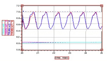
- Re-plot the time-domain signal (purple circle above).,
except change the y-axis to go from 20 to 25 ns to zoom in as
below:
- Save a snapshot of the unstable time-domain oscillation from
20 to 25 ns as illustrated above, and paste it into your
report. ( P6 )
- Estimate the
frequency of the oscillation from the time-domain
oscillation plot? ( Q10 )
- Because of the potential for oscillation in non-Foster
circuits, one should always run a time-domain simulation to
check stability.
- Return the resistors R42 and R43 to 500 ohms
- Set R44 to 100 ohms to cancel the -100 ohm parasitic
resistance
- Rerun the simulation
- Plot the new Smith chart ( P7 )
- Zin1 should now be within the "normal region" of the Smith
chart
- However, is the circuit now stable? yes/no ( Q11 )
- Load and run the CMOS non-Foster circuit example as follows:
- Go down through the directory tree to cmosDiffLinvill_a and
double click that design file, and the following
schematic should appear.
- NOTE/WARNING: for simplicity
and expedience, the high voltage supply was retained from the
BJT design, however, you could not
exceed 5V supply in "real" 0.5 micron CMOS design.
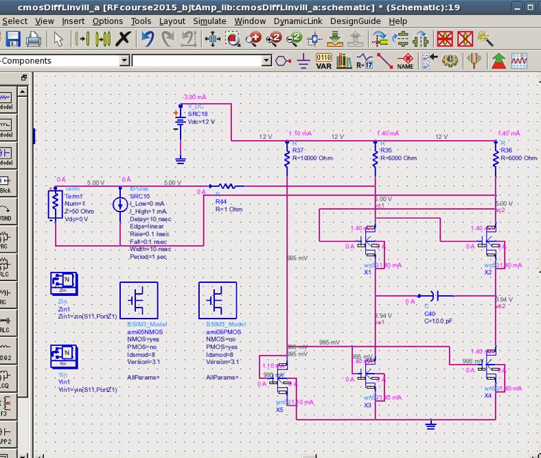
- Run the simulation, and annotate the
dc voltages on the schematic, using
MenuBar::Simulate::AnnotateDc. Save a snapshot of
the schematic and paste it into your report.
( P8 )
- As before,
- For the CMOS circuit, save a snapshot of the real and
imaginary parts of Zin (red circle above), also with 2 markers at 50
MHz as illustrated above. ( P9
)
- For the CMOS circuit, what is the real part of input
impedance Zin1 at 50 MHz (red arrows above)? ( Q12 )
- For the CMOS circuit, what is the imaginary part of
input impedance Zin1 at 50 MHz (red arrows above)? ( Q13 )
- For the CMOS circuit, what is the effective negative
capacitance corresponding to the imaginary part of input
impedance Zin1 at 50 MHz (red arrows above)? ( Q14 )
- Which is better, the CMOS or BJT non-Foster circuit
above? CMOS/BJT ( Q15 )
NOTE ReportTemplate: Use the Project Report Template
and keep answers to questions on
consecutive sheets of paper with all plots at the end.
Do not add extraneous pages or put explanations on separate
pages unless specifically directed to do so. The instructor will
not read extraneous pages!
Only turn in requested plots (Pxx )
and requested answers to questions (Qxx ).
All plots must be labeled P1, P2, etc. and all questions must be
numbered Q1, Q2, etc. YOU MUST ADD CAPTIONS AND FIGURE
NUMBERS TO ALL FIGURES!!
Copyright 2010-2015 T. Weldon
Cadence, Spectre and Virtuoso are registered trademarks of
Cadence Design Systems, Inc., 2655 Seely Avenue, San Jose, CA
95134. Agilent and ADS are registered trademarks of Agilent
Technologies, Inc.