Microwave Circuits and
Metamaterials
Project 4
Overview
Remain in same project groups for the
semester.
The objective of this project is to design simulate a simple CMOS
amplifier using the Cadence simulator.
NOTE: Use the Project Report Template and keep answers to questions on consecutive sheets
of paper with all plots at the end.
IN NO CASE may code or files be exchanged between students, and
each student must answer the questions themselves and do their own
plots, NO COPYING of any sort! Nevertheless, students are
encouraged to collaborate in the lab session.
Only turn in requested plots (Pxx )
and requested answers to questions (Qxx ).
Part 1
- In this part, design simulate a simple CMOS differential
amplifier using the Cadence simulator.
- Also see:
- Load and run the pulse example as follows:
- Download the following zip-file (you may need to hold down
the shift key while you click on the link):
Cadence file rfproj6cadence2012.zip
- You should have already run the Cadence software in
Project1, so you should have the libraries and basic
folders/directories installed in your linux filesystem home
directory. When you ran the Cadence
software in project 1, As soon as you run Cadence software for
the first time, it will automatically install all NCSU ami06
libraries in your cadence6 directory. The ami06
libraries are used to fabricate in the ON Semiconductor 0.5
micron process through MOSIS.com
Return to the project 1 webpage if you did not do this, or if
you do not have a ~/cadence6/NCSU16 diectory.
- Move the file to your ~/cadence6/NCSU16 directory and
extract the file.
- You should see a new library named rfproj6
- Fix the links in ~/cadence/NCSU16/cds.lib by opening cds.lib
(use the nedit/gedit
editor in linux, gnome::programming::Nedit) and
editing it to add the lines as before.
- you should add the following line near the end of the
file:
- Run Cadence6/Virtuoso6 software. From a Linux
terminal, Cadence6/Virtuoso6 software should be available in
the menu
(Mosaic::Engineering::Electrical::Cadence::Cadence6)
From a PC terminal, you must first open a remote Linux
session,
(Start::AllPrograms::Mosaic::LinuxConnect::ToAnyServer), then
proceed as for a Linux terminal
- Warning on
resistors in Cadence6
ami05_c6_customlib
- In post-2014 installations of the Cadence6
ami05_c6_customlib, the resistors (R50, R100, R1K, etc) may
not function properly in simulations. To correct this
problem, open the schematic of each resistor in the library
and replace the existing resistor in the resistor schematic
with a new resistor from the library NCSUAnalogParts::RLC::res
having the proper value. Then, check and save the
schematic, open the layous, extract the layout, and run LVS to
finalize the change. Then, check and save the resistor
cell schematic, open the layout, extract the layout, and run
LVS to finalize the change. Simulation should run correctly
after this. You may wish to check your repairs to
the library by simulating the dc voltages in a simple voltage
divider.
- Design of a CMOS RF Differential Amplifier:
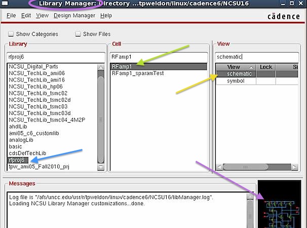
- Once the Cadence/Virtuoso6 software is running, you should
see the library manager window as below, with your new design
loaded in the left pane (blue arrow below)
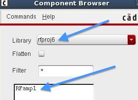
- From library manager, select the rfproj6 library (blue arrow
above)
- Select the RFamp1 cell (green arrow above)
- Select the schematic view (green arrow above) and note the
highlited preview (purple arrow above)
- Double-click the schematic (yellow arrow above) to open the
RFamp1 cell schematic view,
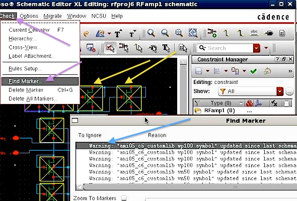
- When first opened you may see yellow warning boxes around
the transistors as shown below.
- If you see the yellow warning boxes as shown above (yellow
arrows above), use MenuBar::Check::FindMarker (purple arrows
above) and in the pop-up box (blue arrow above) make sure the
warnng is as above
- Use MenuBar::File::CheckAndSave and all the yellow warnong
boxes should disappear
- Finally, you should see a schematic as below
- Save a white background version of the schematic as above
and paste it into your report. ( P1 )
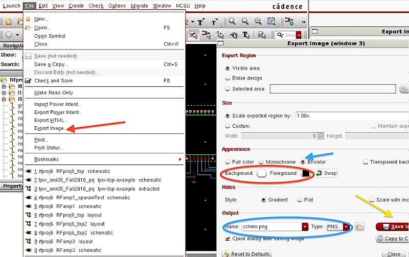
- To export a schematic with white background, use
MenuBar::File::ExportImage (red arrow below) and change the
background to white and foreground black (red circle below),
if desired set bi-color (blue arrow below), enter the file
name (blue circle below) and save the file (yellow arrow
below)
-
- Or even better than a snapshot with a black backgrou
- Make sure that your
plots, component
values,
legends, axes, and fonts are legible in your report! For snapshots use the
Linux menu Graphice::Ksnapshot and select the option
to take a legible snapshot of a window rather than full screen
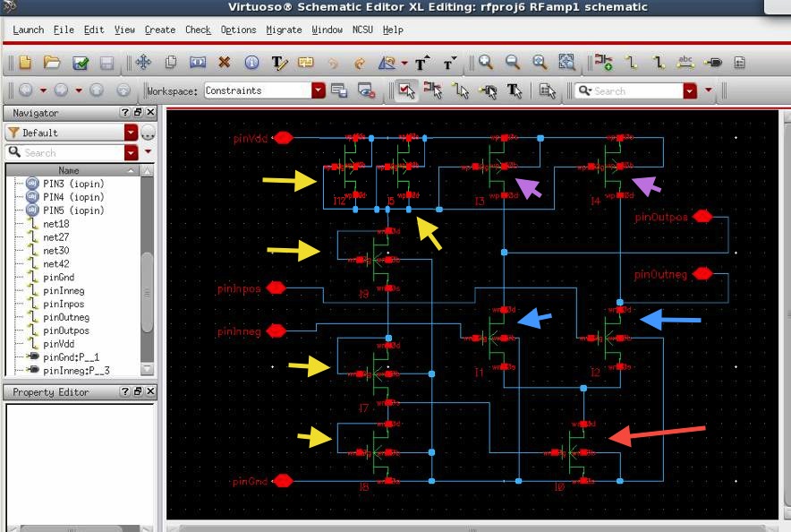
- The 2 pMOS and 3 nMOS transistors in the bias stack on the
left (yellow arrows above) are used to set the bias voltages of the differential
amplifier components on the right of the schematic
- The bottom nMOS in the bias stack is a current
mirror that supplies the gate voltage for the nMOS current source (red arrow above) of
the nMOS differential pair (blue
arrows above)
- Finally, the two pMOS transistors (purple arrows above)
above the differential pair serve as high impedance
current-source loads for the differential pair. (Note:
take care to observe that this is not
an active load as shown on p. 13
of my Review of CMOS and
BJTs
notes)
- Note that the top pair of pMOS transistors (top two yellow
arrows above) in the bias stack split the current, just as the
pair of pMOS transistors (purple arrows above) at the top of
the differential pair split the current from the current
source (red arrow above). Thus, all four pMOS
devices have currents that are half the value of the total
current flowing down through the bias stack.
- The bias stack may be thought of as a voltage divider that
creates bias voltages from the Vdd power supply. The
bias stack may also be thought of as a current-setting device
that establishes useful bias voltages by virtue of the total
current drawn through the devices connected in series in the
bias stack.
- To obtain increased current, wider transistors could be used
in the bias stack.
- In the schematic, note that all nMOS devices have their bulk
terminal to ground, because this is an n-well process where
there is no p-well. The substrate is p-type and serves
as the common bulk or well for all nMOS devices.
- So in your schematics, you
MUST connect all nMOS bulk to ground.
- The pMOS devices do have an n-well bulk, typically connected
to the source.
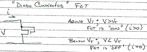
- Review of some basic CMOS structures:
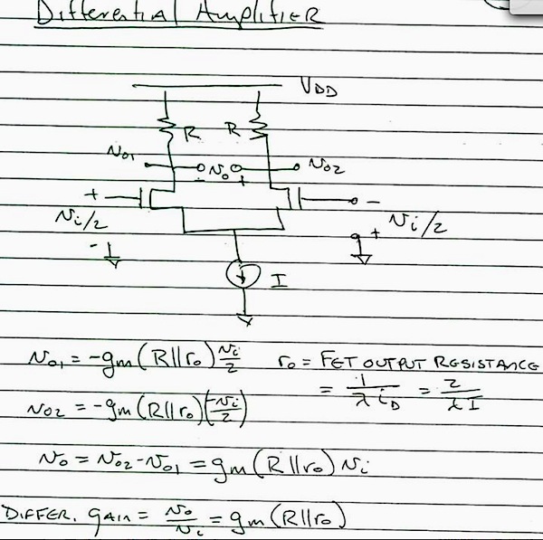
- The bias stack consists of a stack of diode-connected FETs
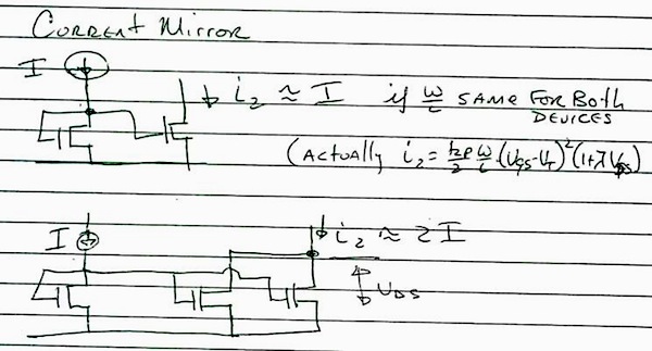
- The basic current mirror structure is as follows:
- The basic differential amplifier structure is:
- In the example circuit in cadence6, RFamp1, the resistors
R shown in the above schematic are replaced by the high
impedances of the 2 pMOS current mirrors to boost gain
(using R=Rds=1/gds of the 2 pMOS devices above the
differential nMOS pair). Note,
however, that the extra external load of 5 kohms in the
test schematic will also be in parallel, and reduce the
gain.
- Another bias scheme, including input bias and decoupling
capacitors is illustrated below:
- Simulating the amplifier:
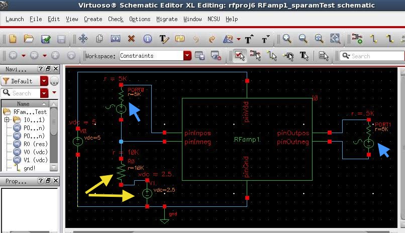
- Next, open the S-parameter test circuit RFamp1_sparamTest,
under the librabry manager cell pane, double-clicking the
schematic, and the schematic should appear as below
- Note the two "psin" ports as before (blue arrows below),
except that they have 5000 ohm
impedance instead of 50 ohms
- The 10,000 ohm resistor and 2.5 volt source (yellow arrows)
provide dc bias at the the differential input
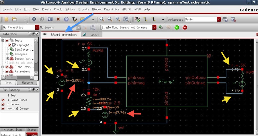
- Save a snapshot of the schematic as above and paste it into
your report (voltage annotations above may be
missing). ( P2 )
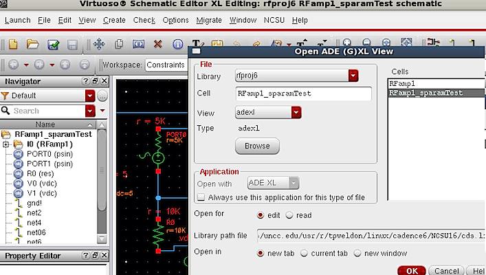
- Launch ADE XL using MenuBar::Launch::ADEXL and open the
existing view as shown below
- In ADE XL, doubleclick the rfproj6:RFamp1_sparamTest:1 test
(purple arrow below) to get the ADEXL test editor window
(purple oval below)
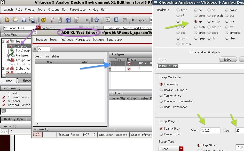
- In the test editor, double-click the "sp" s-parameters (blue
arrow below) to edit and observe the simulation settings
(green arrows below) as shown below
- Similarly, double-click the dc simulation (blue arow below)
in ADE XL and observe the setup
- Especially note the options button (red arrow below)
and "Save DC operating point" item (left yellow arrow below)
and "all" item (right yellow arrow below)
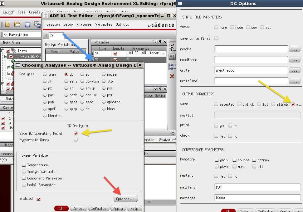
- The DC Options window appears after clicking the options
button (red arrow below)
- The "all" setting and "DC operating
point" (yellow arrows below) are needed to later annotate
the schematic with dc voltages from simulation
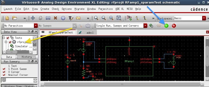
- As before, run the simulation (blue arrow below)
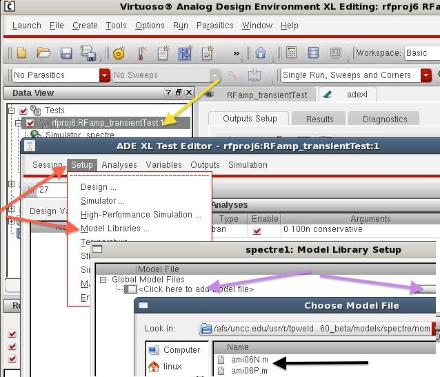
- See note below the schematic if you get an error regarding
model libraries or ami06N.m or
/afs/uncc.edu/usr/r/tpweldon/linux/cadence6/ncsu_cdk_160_beta/
- If you get an error regarding
missing model libraries such as:
- Unable to open input file
`/afs/uncc.edu/usr/r/tpweldon/linux/cadence6/ncsu_cdk_160_beta/models/spectre/nom/ami06N.m'
- Then,
- you must double-click the test (yellow arrow below) and
"OpenTestEditor"
- in the TestEditor run
MenuBar::Setup::ModelLibraries (red arrows below)
- Delete the offending libraries, and add the correct
libraries (purple arrows below)
- Add the nMOS and pMOS librbaries (black arrows below)
- As before, link to your own libraries
~/cadence6/ncsu_cdk_160_beta/models/spectre/nom/ami06N.m
and ami06P.m
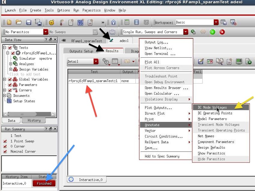
- Select the ADEXL tab and results tab (black arrows
below), if these two tabs are not already selected after
simulation runs
- After the simulation finishes (blue arrow below),
right-click the test (red arrow below), and select
Annotate::DCnodeVoltages (yellow arrow below)
- The schematic will appear with the annotations, click the
ADEXL tab (black arrow below) to return to the ADEXL frame
- Similarly, right-click the test (red arrow below) and
select Annotate::DcOperatingPoint to add the currents to the
schematic, too.
- The annotated schematic should appear. Click the
schematic tab (blue arrow below) if the schematic does not
appear automatically
- The dc voltages (yellow arrows below) should appear on the
schematic
- The dc currents of voltage sources (red arrows below) should
appear on the schematic
- Save a snapshot of the annotated schematic showing both voltages and currents as
above and paste it into your report. ( P3 )
- What is the dc current supplied to the "pinVdd" pin of the
RFamp1 circuit? (Q1 )
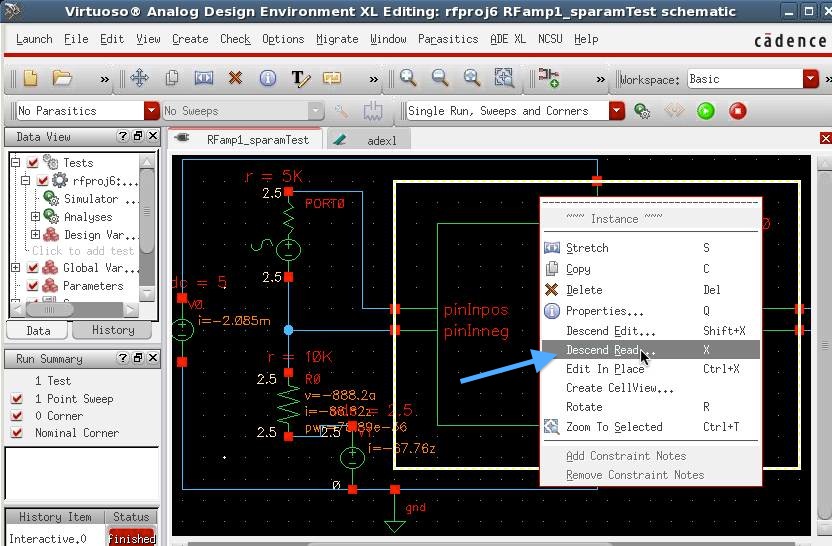
- On some cells, the dc voltage annotation will also appear in
subcircuit schematics. However, in most cases this
appears not to be true (possible bug).
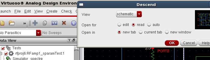
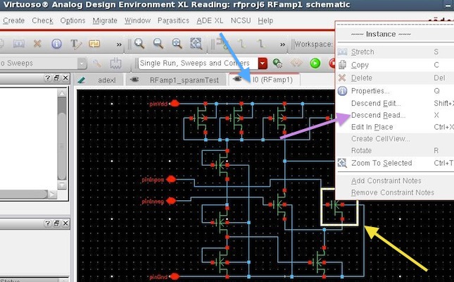
- As shown below, to check the RFamp1 subcircuit, right-click
the RFamp1 symbol in the test schematic, and DescendRead (blue
arrow below) to see if the voltages were annotated
- Most likely the voltages were not annotated (there seems to
be a bug here)
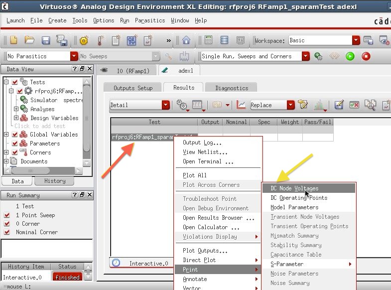
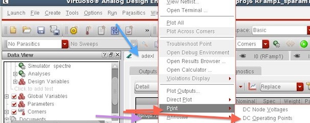
- As a workaround, we can use a slightly different procedure
to read the dc voltages
- Right-click the test (red arrow below) and select
Print::DCnodeVoltages (yellow arrow below)
- A results display window (red arrow below) should pop up
- Click on nodes of the subcircuit (yellow arrows below) and
the corresponding dc voltages should be printed in the results
window (blue arrows below)
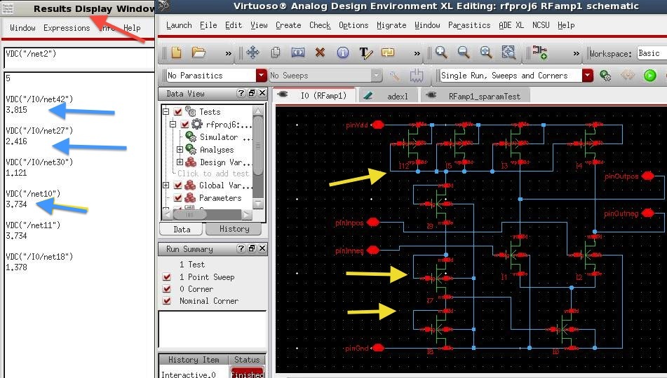
- Save a snapshot of theRFamp1 schematic adding all 7 dc node voltages
to the schematic paste it into your
report. ( P4 )
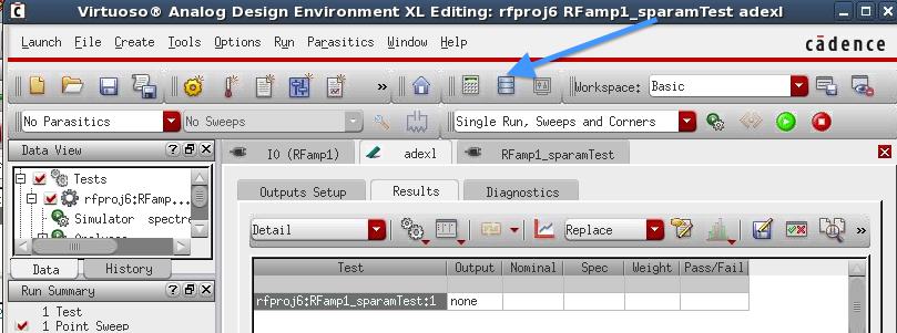
- To plot the S-parameters, click the results browser button
(blue arrow below) on the ADE XL toolbar
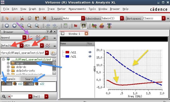
- In the visualization window that pops up, select the
S-parameters, and S11 and S21holding down shift or control key
to be able to highlight both (blue arrows below)
- Select default or rectangular and db20 (red arrows
below) to plot the S-parameters in log scale from 0 to 2
GHz
- Press the PlotSignals button (purple arrow below)
- Change the plot to a white background (right-click inside
plot and select properties), and thick lines (double-click the
lines), one dashed and one solid (yellow arrows below) as
shown below
- Save a snapshot of the S11 and S21 as above and paste it
into your report. ( P5
)
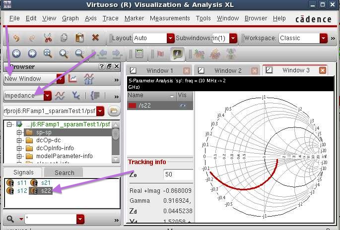
- Finally, plot S22 on a Smith chart (purple arrows
below) with a thick line
- Save a snapshot of the S22 Smith chart as above and paste it
into your report. ( P6
)
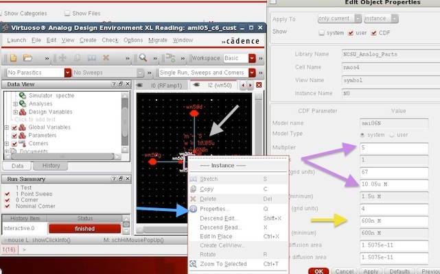
- Select the schematic of the amplifier (blue arrow below)
- Right-click the nMOS transistor on the right side of the
differential pair (yellow arrow below)
- Select DescendRead (purple arrow below)
- In the schematic of the device, right-click the device anc
click Properties (blue arrow below)
- In the properties window, note the size parameters of this
wn50 nMOS device
- The device gate length is 600 nm (yellow arrows below)
- The device consists of 5 fingers that are 10.05 um long
(purple arrows below) for a total effective gate width of
approx. 50 um
- Note also that the same information appears on the scheatic
(gray arrow below)
- Return to the ADEXL tab where your simulation results are
shown (blue arrow below)
- Select the test run (purple arrow below) and right-click to
select Print::DcOperatingPoint (red arrows below)
- A pop-up window (yellow circle below) should appear
- Select the tab with your lowest-level single transistor
schematic (yellow arrow below)
- Click the transistor body to print out the operating point
as below
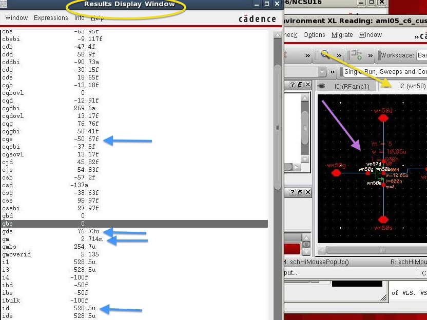
- Record the nMOS transistor's values for gm, gds (equals
1/Rds), and Cgs (blue arrows above), and record these in your
report.
(Q2 )
- Repeat the process for the pMOS load transistor directly
above this nMOS transistor, and record these in your
report.
(Q3 )
- Based on the theory above, differential voltage gain would
equal gmn*(Rdsp||Rdsn) if the 5 kohm external load was not
present, where gmn is gm of the nMOS device, and Rdsp is the
Rds=1/gds of the pMOS device acting as the load, and it is
seen in parallel with Rdsn of the nMOS device. For your
circuit, what is gmn**(Rdsp||Rdsn) in dB (use 20 log10)? (Q4 )
- When your differential external load in the test circuit of
5000 ohms is included, it acts as two loads of 2500 ohms
connected to virtual ground and in parallel with Rdsp.
So the effective differential voltage gain becomes gmn*Req,
where Req is Rdsp||Rdsn||2500, or Rdsp in parallel with Rdsn
in parallel with 2500. For this resistance, calculate
the gain gmn*Req in dB in dB and compare it to S21 of your
simulation S21. (Q5 )
- Note: you will see a 6 dB discrepancy
in gain compared to S21, because the input impedance
is not matched (it is nearly open circuit resulting in double
the voltage of a matched load at the input).
- What is the 3 dB bandwidth of your amplifier? (Q6 )
Part 2
- Next, a transient analysis will be done
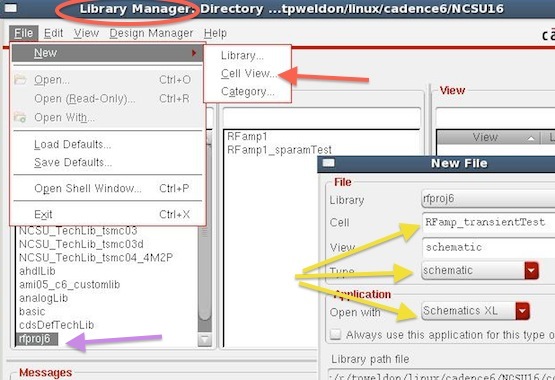
- Select in the rfproj6 library in the library manage as shown
(purple arrow below)
- Create a new cell schematicXL view from LibraryManager
MenuBarFile::New::CellView(red arrow)
- Name the new cell RFamp_transientTest of type schematicXL
(yellow arrows below)
- Enter a transient pulse test schematic as (see the figure
after the next one)
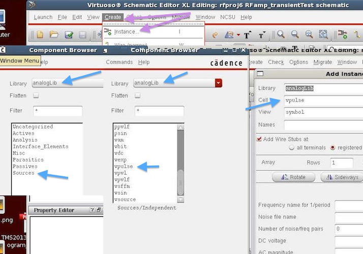
- To begin, first add a pulse generator instance of vpulse
using the MenuBar::Create::Instance (purple arrows below) in
the schematic editor.
- In the popup componentBrowser select analogLib at the top
(topmost blue arrows below) and navigate through
analogLib/sources/independent hierarchy to find vpulse (blue
arrows below) and the AddInstance will popup, at which
time you can click on a schematic to place the component
- Next, repeat the MenuBar::Create::Instance procedure adding
a new Instance of two 10,000 ohm resistors (red arrows below),
from the analogLib/Passives/res
- Next, repeat the MenuBar::Create::Instance procedure adding
a 2.5 volt dc source, and a 5 volt dc source, from
analogLib/Sources/independent/vdc
- Next, repeat the MenuBar::Create::Instance procedure adding
a ground, from analogLib/Sources/globals/gnd
- Next, repeat the MenuBar::Create::Instance procedure adding
a copy of your circuit , from rfproj6/RFamp1 as shown below
- Wire the circuit (blue circle below) as shown below
- Right-click each device and select properties to set the
values correctly, as noted above
- Add the 4 wire names "vinPos," "vinNeg," "voutPos,"
"voutNeg" (blue arrows below) by using the toolbar button
(black arrow below)
- Beware: the menu may hide behind your schematic after each
use
- CheckAndSave your schematic (red circle above)
- Save a snapshot of the schematic as above and paste it into
your report. ( P7 )
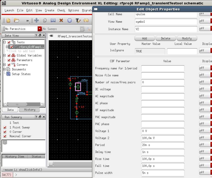
- Select the vpulse, type "q" on the keyboard, and set the
vpulse properties as below:
- CheckAndSave your schematic
- Launch ADE XL using MenuBar::Launch::ADEXL and create a new
view (type adexl) as shown below
- In ADE XL, click below tests (blue arrow below) to add a new
test, choose your new RFampTransient designitem in the
popup, and this should open ADE XL test editor shown below
- Click MenuBar::Analysis::Choose (red arrow below) and
setup a transient analysis for 100 ns as shown below.
- As before, use MenuBar::Setup::Models to add the nMOS and
pMOS models
- link to your own libraries
~/cadence6/ncsu_cdk_160_beta/models/spectre/nom/ami06N.m and
ami06P.m
- See the detailed description earlier on this webpage,
describing the steps outlined in the following picture
- s
- Finally, make sure to save all of
your test settings from within ADE-XL.
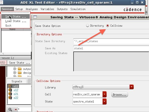
- Use MenuBar::Session::SaveState from within TestEditor as
shown below
- Make sure to save the state in the
CellView (red arrow below)
- Note: If you closed Test Editor and the window is not
open, you can reopen it by right-clicking the test item
under "Tests" in "Data view" pane on the left side of the
ADEXL window
- Note: from within ADEXL there is a second type of saving
an overall ADEXL state from the ADEXL MenuBar as
MenuBar::File::SaveSetupState It does not appear that this
second type of saved state saves the test setup of the
test editor pane
- Next, add the outputs using the toolbar button (red arrow
below) or MenuBar::Outputs::Setup
- Select the FromSchematic option (blue arrow below)
- Add the four named wires so they appear in the test editor
outputs pane (yellow arrows below)
- Use MenuBar::Session::SaveState from within TestEditorto
save your session as before (overwrite)
- Run the simulation using the RunSimulation button (blue
arrow below)
- The plot all the signals using the PlotAllWaveforms
button (red arrow below)
- Plot the four signals from 0 to 100
ns as illustrated in the slightly different plot
below in the visualization window
- Change the plot to a white background, and thick lines, as
shown below
- Save a snapshot of the transient simulation as above (except
only for 100 ns) and paste it into your
report. ( P8 )
- What is the differential voltage gain (linear ratio
vout/vin) of RFamp1 as estimated from the transient
simulation? Use the differential pulse voltages, even
though the input may not be balanced. Hint: use markers
to more accurately measure the voltage changes and voltages.
(Q7 )
- What is the voltage gain in
dB of RFamp1 from the transient
simulation? (Q8 )
- If you close all your simulation and schematic windows, you
should be able to return to the test setup by vlicking on the
adexl view for your cellviews for transient and S-parameters.
- In the IEEE Microwave Symposium Jul 1991 paper "Recollections
on
microwave theory ," N. Marcuvitz describes in 1941
at MIT how they used their hands or cheeks to determine if
microwave energy was coming down a waveguide. This was before
high frequency detectors were widely available. (Note that
cellphones were in wide use 50 years later!) For even
greater sensitivity than the cheek, what part of their
face did they use to sense microwaves? (
Q9 )
- Exit the program, File::Exit
For further details see the supplement project04_s15xtraSparamsFromScratch.html
that goes over details on:
- Creating a schematic from scratch using the ami05_c6_customlib
library
- Setting up S-parameter tests from scratch using ADEXL software
- Creating a symbol for a schematic/design
- Using components from the library supplied in class,
ami05_c6_customlib library
NOTE ReportTemplate: Use the Project Report Template
and keep answers to questions on
consecutive sheets of paper with all plots at the end.
Do not add extraneous pages or put explanations on separate
pages unless specifically directed to do so. The instructor will
not read extraneous pages!
Only turn in requested plots (Pxx )
and requested answers to questions (Qxx ).
All plots must be labeled P1, P2, etc. and all questions must be
numbered Q1, Q2, etc. YOU MUST ADD CAPTIONS AND FIGURE
NUMBERS TO ALL FIGURES!!
Copyright � 2010-2015 T. Weldon
Cadence, Spectre and Virtuoso are registered trademarks of
Cadence Design Systems, Inc., 2655 Seely Avenue, San Jose, CA
95134. Agilent and ADS are registered trademarks of Agilent
Technologies, Inc.